

Confinement strategy for oriented growth of Mo6Te6 NWs
Thermal annealing of TMDs is widely used in fabricating TMC-NWs in the reported synthesis strategies17,18,21. When annealing is applied to the unconfined MoTe2 flakes, Te vacancies are generated throughout the flake, leading to the random in-plane nucleation of NWs. With continuous heating, NWs grow freely along different zigzag directions of the original lattice, which leads to the formation of a disordered NW network as demonstrated in the schematic of Fig. 1a, c.

a–c Schematics of the conversion of disordered NWs through applying thermal annealing. d–f Schematics of the conversion of oriented NWs in the graphite-encapsulated 2H-MoTe2. Potential Te migration pathways in a graphite-confined MoTe2 flake are highlighted by orange arrows in (e) including 1) penetrating graphite layers, 2) along NWs, and 3) along the gaps between NW bundles.
To regulate the growth orientation of Mo6Te6 NWs to achieve oriented patterning, random in-plane nucleation must be restrained. Encapsulation experiments23 and theory24 show significant energy barriers for traversing the graphene hexagonal lattice even by small atoms like He and H. Inspired by this, we propose that confining the MoTe2 flake with graphite layers may restrict the generation of Te vacancies and also their migration pathways. Thus, the confining strategy may change the random in-plane nucleation of NWs to confined nucleation at the edge and would achieve the regulation of the growth orientation from isotropic to along certain specific orientations, as indicated in the schematic of Fig. 1d, f.
In-situ electrical-bias-induced oriented NWs growth in MoTe2
Phase transitions can be realized by introducing various external stimulations in TMDs8,25,26. To verify the above-proposed strategy, we apply in-situ electrical bias to a freestanding graphite-sandwiched 2D MoTe2 heterostructure and simultaneously record its structural evolution in a STEM. Figure 2a presents the schematic diagram of the heterostructure, fabricated on a commercial microelectromechanical-system (MEMS) chip with the corresponding current flow when an electrical bias is applied. A detailed optical-microscope image of such a heterostructure is shown in Suppl. Figure 1. The heterostructure is fabricated using a polycarbonate (PC) microdome transfer method conducted by a 2D transfer platform (Suppl. Figure 2), while the few-layer graphite and MoTe2 flakes are prepared by a standard scotch-tape cleavage method (see “Methods”). Since MoTe2 is sensitive to oxygen, all sample fabrications are conducted in a nitrogen-protected glove box to prevent contamination and oxidation. The top and bottom graphite layers in the heterostructure are connected to the electrode that is prefabricated on the MEMS chip, which generates a uniform electric field in the heterostructure region where MoTe2 has graphite on both sides. Moreover, the top and bottom graphite electrodes are sufficiently thin so that they do not disrupt the atomic imaging of the MoTe2 structural evolution.

a Schematic depiction of the graphite-MoTe2-graphite heterostructure device on the in-situ microelectromechanical system (MEMS) chip. The graphite layers on the top and bottom are connected to the positive and negative electrodes of the chip, respectively. The current flow is highlighted by black dashed arrows, and the electrodes on the MEMS chip is highlighted by yellow. b–d A series of high-angle annular dark-field (HAADF) scanning transmission electron microscopy (STEM) images showing the dynamic growth of the oriented NW bundles. White arrow indicates surface undulations as reference marker during structure conversion. e The evolution of resistance as a function of time measured through the chip during the in-situ experiment with the schematic indicating the phase transition inserted. A rapid drop in resistance and the growth of NWs were observed simultaneously when the voltage reached 2.5 V. f, g Cross-sectional HAADF images of the 2H-MoTe2 (f) and the as-grown Mo6Te6 NW bundle (g). h, i Zoom-in atomic images showing the clean interface of 2H-MoTe2/graphite (h) and Mo6Te6/graphite (i) with the atomic models overlaid. Source data are provided as a Source Data file.
Figure 2b, d shows a series of low-magnification high-angle annular dark-field (HAADF)-STEM images taken at different stages of the oriented growth of Mo6Te6 NWs. Figure 2b is acquired before applying the bias voltage. We confirm that the sample is 2H-MoTe2 by the HAADF image (Suppl. Figure 3). By slowly increasing the applied bias voltage to 2.5 V, a stripe-like 1D structure is suddenly observed at the sandwiched heterostructure edge and keeps extending into the middle region of the hole when maintaining the bias voltage. Although slight deflection of certain stripes is observed due to surface undulations (see Suppl. Figure 4), most of the stripes’ growth direction remains unchanged (see Fig. 2c). By further increasing the applied bias voltage to 4 V, the growth of the new structure becomes faster along the same growth direction (see Fig. 2d). Additional selected area electron diffraction (SAED) and Raman spectra confirm the conversion of 2H MoTe2 into Mo6Te6 NWs, as shown in Suppl. Figure 5, 6.
Figure 2e shows the corresponding time-resistance curve record by the MEMS chip during the STEM imaging process in Fig. 2b, d. As can be seen, when the bias voltage reaches 2.5 V, a relatively large drop in resistance is observed. This indicates that a structural-transformation-induced resistance drop occurred in our experiment. It should be noted that below 2.5 V, when bias voltage is stable, the resistance remains constant (see Suppl. Fig. 7), suggesting that an activation threshold of voltage (in our case 2.5 V) is required for the formation of NWs.
To determine the structural changes of MoTe2, we use a focused ion beam (FIB) to make a cross-sectional sample near the as-grown structure in the region marked by a red rectangle in Fig. 2d. The thicknesses of the top and bottom graphite layers are 5.7 and 5.9 nm, respectively, while the MoTe2 film is 15.8 nm (Suppl. Fig. 8). Figures 2f, g shows cross-sectional HAADF images of the original 2H-MoTe2 and the converted Mo6Te6 NW bundles. The conversion of a 2D flake to 1D bundle does not generate much volume change, mainly due to the confinement effect between the graphite electrodes. Zoom-in images of the interface between graphite/MoTe2 and graphite/Mo6Te6 NW are shown in Fig. 2h, i with the atomic-lattice model overlaid, respectively. MoTe2 is in perfect 2H stacking in which the orientations of the prismatic unit cells are inverted between layers, while the converted NWs also maintain a close-packed bundle structure as reported in ref.21. Moreover, the interface between the confined graphite layers and MoTe2 is atomically flat (Fig. 2h), demonstrating the high cleanliness of our transfer method, as no contamination is introduced into the interface during the sample preparation process. It is assumed that the flat interface generates a uniform vertical electric field when an in-situ electric bias is applied. Such a flat interface is preserved during the conversion, indicating a rapid reaction process. Meanwhile, because of the different unit cell parameters of 2H-MoTe2 and Mo6Te6 NW (c axis of Mo6Te6 NWs is around 7.6 Å and 2H-MoTe2 is 7 Å)21, mismatching is present between 2D layers and 1D NWs at the lateral connection (Suppl. Fig. 9). The oriented growth behaviour of NWs remains consistent across varying thicknesses of graphite and MoTe2 layers, as long as the MoTe2 is graphite-confined on both sides (see Suppl. Fig. 8b for another device with different thickness of graphite layers).
Because bulk Mo6Te6 NWs are metallic21, the appearance of NWs in MoTe2 reduces the resistance of the device, which explains the sudden resistance drop in Fig. 2e. Furthermore, the X-ray energy-dispersive spectroscopy (EDS) results also confirm that the Mo:Te composition of the stripe-like structure is about 1:1 (Suppl. Fig. 10), indicating the complete conversion from 2D MoTe2 to 1D Mo6Te6 NWs.
In-situ STEM study of the oriented growth of Mo6Te6 NWs
To understand the structural conversion from 2H-MoTe2 to Mo6Te6 NWs, we investigate the dynamic growth of Mo6Te6 NWs by in-situ STEM characterizations. Figures 3a, b shows the optical microscope image and the zoom-in HAADF-STEM image of a free-standing hole region of the graphite-sandwiched MoTe2. In Fig. 3b, the red line represents the edge of the top-layer graphite flake (depicted in Fig. 3c). Note that in the region where MoTe2 is covered by graphite on both sides (above red line), oriented bundle-like Mo6Te6 NWs are converted from MoTe2 under bias modulation. However, the lack of double-sided graphite coverage of MoTe2 (below the red line) result in an amorphous film composed of random size Mo-rich clusters, as shown schematically in Fig. 3d (structure and EDS results are shown in Suppl. Fig. 11).

a Optical microscope image shows the geometry of the graphite sandwiched MoTe2 heterostructure. The top and bottom graphite are marked by red and black outlines, respectively, while the MoTe2 film in between is marked by a blue outline. Highly oriented growth of NWs was observed in the freestanding hole on the chip indicated by a dashed black circle. b Zoom-in low-magnification HAADF-STEM image taken at the heterostructure region where MoTe2 is covered by graphite on both sides, within the area indicated by the blue box in (a). Bundle-like structure, namely Mo6Te6 NWs, is seen in the region that is fully sandwiched between the graphite sheets (above the red line). Below the red line, absent the graphite sheets, MoTe2 is converted to amorphous film composed of random size clusters. c, d Schematics of the structural transition from the graphite confined 2H-MoTe2 to Mo6Te6 NWs before and after applying electrical biasing within the area indicated by the green box in (b). The area shaded in grey is the heterojunction region with the graphite edge marked by a red line. The MoTe2 film that is not sandwiched in graphite sheets in the blue area of (d) is converted into amorphous film composed of clusters. Series of (e) high- and (f) low-magnification HAADF-STEM images that taken during the conversion of 2H-MoTe2 into Mo6Te6 NWs. The MoTe2 (110) and (100) facets are highlighted by white and yellow dashed line in (e) and (f), and the growth direction of NWs is highlighted by white arrow in (e).
During the growth of oriented NWs, a series of high-resolution STEM images are taken at the growth frontier of the NWs bundles as shown in Fig. 3e, which clearly indicates that the growth direction of Mo6Te6 NWs is along specific zigzag edge ((100) facet) of 2H-MoTe2. Figure 3e also reveals that the NWs remain terminated at the (110) facet of the 2H-MoTe2 during the growth. Moreover, the interface is quite sharp without Moiré overlapping patterns, indicating a rapid and complete phase transition under the electrical biasing.
To unveil the dynamical behaviours of NWs at a larger scale, Fig. 3f shows a series of low-magnification STEM images. The lateral connection between Mo6Te6 NW and MoTe2 is steplike. We observe in Fig. 3e that the MoTe2 (110) facet, where NWs are terminated, is continuously transformed into Mo6Te6 NWs, leaving the (100) facet exposed and elongated. In other words, the growth of the NWs does not deflect due to such special growth behaviour. Instead, as the NW grow, MoTe2 is selectively consumed at the (110) facet so that the NWs can elongate only along the edge of the MoTe2 (100) facet. Note that the conversion is not 2D-to-2D as gaps with random widths can be observed between NW bundles. The formation of these gaps is because almost half of the Te atoms in MoTe2 are ejected during the structural transformation from MoTe2, which results in a huge volume reduction relative to the initial state.
Graphite confinement effect and growth mechanism
To interrogate the confinement effect of the graphite layers step by step, we first conduct controlled in-situ heating experiments. The thickness of the top and bottom graphite layers is around 15 and 20 nm for MoTe2. The results are shown in Fig. 4a, b and Suppl. Figs. 12, 14. We find that global heating also converts the double-sided graphite-confined 2D MoTe2 flake into oriented NWs at 600 °C. However, incomplete conversion where MoTe2 and NWs have substantial overlaps is observed at the contact region (pointed by yellow arrows in Fig. 4a; more information is shown in Suppl. Fig. 13), while the conversion is quite sharp at the electrical biasing case (Fig. 4c, d and Suppl. Fig. 12). The difference in the interface structure in these two experiments may be caused by different heating treatments. As current flows through the converted NWs region and induces local joule heating, the electrical biasing may engender more localized defect generation at the interface, while direct heating can be considered as more global. We also find that changing the bias voltage and heating temperature (above threshold value) will only result in altering the growth speed of NWs, as illustrated in Suppl. Fig. 16, higher temperature will have faster growth rate than the electrical bias experiment (detailed growth rate shown in Suppl. Figs. 15e, f). Without graphite confinement, the MoTe2 film turns into a layer of mixed disordered NWs and Mo clusters upon electrical biasing (Fig. 3b) or heating (Suppl. Fig. 14), consistent with ref.21.
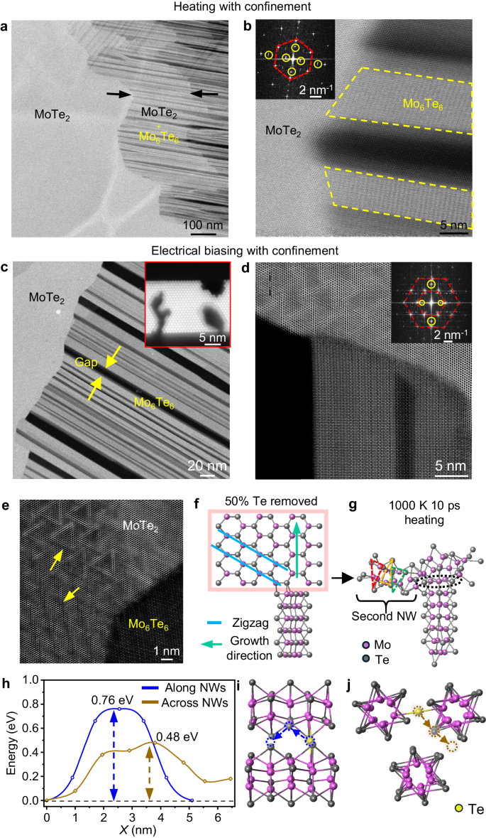
Low (a and c) and high-magnification (b and d) HAADF-STEM images showcasing the conversion of Mo6Te6 NWs from 2H MoTe2. a,b 2H phase region overlap can be observed in heating with confinement, with the FFT pattern inserted in (b) (the FFT patterns highlighted by red dash line and yellow circle representing the 2H MoTe2 and Mo6Te6 NWs). c,d. The interface structure in electrical biasing is clean and sharp. The inserted images in (c) showcase the cross-sectional HAADF-STEM images of the gap structure in the NW region. The inserted image in (d) is the FFT pattern corresponding to the STEM image in (d). The FFT pattern regarding to 2H MoTe2 and Mo6Te6 NWs are highlighted by red dash lines and yellow circles. e High-resolution STEM image showing triangular- and line-shaped defects formed in the MoTe2 region (yellow arrows) near the growth frontier during electrical biasing. f–j MD simulation of the Mo6Te6 NW formation in a MoTe2 lattice with Te deficiency. h DFT-calculated energy barrier for a Te atom migrating along and across three close-packed Mo6Te6 NWs (blue and brown line highlighted). The migration energy barriers are calculated by changing the x-axis coordinate of the Te atoms. (x= The horizontal coordinate position of the Te atom relative to its starting point along the migration path, with the origin set at the initial position of Te in the supercell). The corresponding schematics are shown in i,j. Source data are provided as a Source Data file.
The formation of the MoTe2-graphite interface in the heterostructure is also crucial in this transition. Firstly, after fabricating the graphite-encapsulated MoTe2 heterostructure, two metal-semiconductor Schottky barriers form at the contact interfaces due to the different work function of graphite and MoTe227,28,29,30,31. The applied electrical bias will therefore, induce a forward and reverse bias on the two Schottky barriers and generate Joule heating at the reverse-biased interface. In this case, the Te vacancies can then be generated in the part of the MoTe2 layer that is close to the lower graphite sheet when a critical bias is reached (sufficiently high temperature by Joule heating). The formation of vacancies is confirmed by the presence of complex defect patterns at the growth frontier at the MoTe2 side near the MoTe2/NWs interface, as shown in Fig. 4e. Such complex defect patterns have been shown to be generated when Te vacancies are created by vacuum annealing32. The corresponding NWs growth schematic induced by Joule heating is shown in Suppl. Fig. 16. It is also notable that unlike prior work that obtained transformations of MoTe2 to other phases by vacancy generation8,18,21,26,33,34,35,36,37, we only observe the direct transformation to oriented NWs, most likely because of the unique heterostructure we use to confine the material.
It seems that vertical conversion of NWs is more thorough in the electrical biasing case (detailed discussion in Suppl. Fig. 16), as a sharp MoTe2/NWs connected interface is always present (Figs. 3e and 4c, d), while an overlapping interface is persistently seen in the case of global heating (Figs. 4a, b), presumably due to localized vs. global heating conditions. We also notice that in either electrical biasing or confined heating experiments, no particles or clusters of the escaped Te atoms are observed. We infer that, when the escaped Te atoms enter the gaps (NWs region), they are more likely to migrate along the gap and rapidly vaporize from the heterostructure inside the ultra-high vacuum of the microscope.
To further elucidate the defect-induced formation of NWs, molecular dynamics (MD) simulations based on density functional theory (DFT) are performed. Figure 4f, g shows the process of simulating the Mo6Te6 NW formation in which a single NW is placed against a 2H-MoTe2 monolayer (see Suppl. Fig. 17 for a single NW facing a slanted zigzag edge). To simulate the Te defects generated by the bias voltage during experiments, we artificially removed 50% of the Te atoms in MoTe2. After that, by placing the structure at 1000 K, after 10 ps, a Mo3Te3 ring is found at the head of the pre-placed NW, as shown in Fig. 4g. This MD result indicates that under the conditions of heating and high concentrations of missing Te atoms, NWs can grow along the MoTe2 vertical zigzag direction (red lines in Fig. 4f). The slanted zigzag edge (blue lines in Fig. 4f) is part of the growth process because it is the energetically favoured edge, as revealed by DFT calculations (the energy density is 0.26 \({{{\rm{eV}}}}{\mathring{\rm A} }^{-1}\) for zigzag edges but 0.40 \({{{\rm{eV}}}}{\mathring{\rm A} }^{-1}\) for armchair edges).
Figure 4h present potential energy barriers for the migration pathways shown in Fig. 1c. The detailed schematic regarding these two migration paths is shown in Fig. 4i, j. The diffusion energy barrier for Te atoms migrating along NWs (Fig. 4i) is 0.76 eV (0.69 eV on a single NW, Suppl. Fig. 18) and 0.48 eV (Fig. 4j) for migrating laterally to the gaps, which is even lower than along the NWs. These relatively small energy barriers ( < 1 eV) enable migration at room temperature and suggest that, even more so in the heated environment of the experiment, the ejected Te atoms tend to migrate laterally and finally accumulate within the void spaces among NW bundles. When Te atoms enter the gaps, they may either condensate to form droplets or wet the void spaces. DFT calculations find that the total energy of Te adhere to a single NW is 0.5 eV higher than that of Te in the bulk, signifying a repulsive interaction with the NWs. Considering that the growth of NWs originates from the edge of the heterostructure, these gaps can connect the newly exposed MoTe2 edge to the vacuum chamber in the STEM, enabling Te atoms to migrate freely along the gaps and away from the heterostructure.
Contact properties of Mo6Te6 NW based devices
An isolated Mo6Te6 NW is an indirect bandgap semiconductor13, while bulk Mo6Te6 NWs exhibit a partially occupied conduction band, indicating their conductive nature as proper contact candidates to TMDs devices21. Using the same confined strategy revealed by the atomic STEM results, we directly pattern NWs on devices and measure their contact performance. Figure 5a shows the linear I–V curve of the patterned NW bundles, and the inset of R–T measurement confirms its metallic characteristic. We deposit metal electrode arrays on the patterned Mo6Te6 NWs to measure the contact resistance at the metal-NW interface. We choose four metal deposition recipes to estimate the conducting nature of the NWs as contact. Figure 5b illustrates the linear curves of resistance vs. channel lengths at interfaces between NWs and Au + Ti, Au + Cr, Cr + Ti, and Pd + Ti electrodes, where Ti or Cr often serve as adhesion layers with a thickness of approximately 6 nm38,39. Among these four combinations, gold electrodes exhibit minimal contact resistance ( ≈ 43.7 Ω µm for Au + Cr and 88.4 Ω µm for Au + Ti). The low contact resistance is possibly attributed to the conductive nature of the NWs and the close contact formed between the deposited metal electrodes and the NWs (bundle structure with random gaps) compared to traditional metal-2H or metal-1T’ contacts.
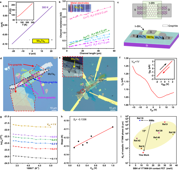
a Transfer curve (Ids−Vds) of Mo6Te6 NWs device, showing linear behaviour. The inserted R-T curve demonstrates the metallic nature of bulk Mo6Te6 NWs. b Contact resistance between Mo6Te6 NWs and Au+Ti, Au+Cr, Cr+Ti, and Pd+Ti metal electrodes. The Ti and Cr metal are deposited as adhesion layer with thickness around 6 nm. c Schematic of our NWs-MoTe2-NWs FET device. d Optical-microscope images of the fabricated graphite confined MoTe2 heterostructure, and (e) the fabricated FET device. We introduce graphite confinement and fabricated oriented NWs at both ends of the MoTe2. An optical-microscope image confirming the conversion of oriented NWs at the graphite edge is shown in the inserted image in (e), (f) Transfer curve (Ids−Vgs) at Vds = 1 V, with Ids−Vds characteristics of the device at room temperature with gate voltage (Vgs) = 0 inserted, showing linear behaviour. g Arrhenius plot ln(Ids/T3/2) versus 1000/T at different values of Vds (T vary from 300–200 K). h Extraction of qΦB via the intercept value, where each data point represents the slope obtained from the Arrhenius plot in (g) using a specific value of Vds. i Comparison of contact resistance between 1 T’/NWs-metal electrodes and Schottky barrier height of the 1 T’/NWs-2H contact FET of this work with the previous reported results8,9,16,18,21,36,40,41,42,43,44. The devices with 1 T’−2H MoTe2 contact are highlighted in the yellow ellipse, while NW-2H contact devices are highlighted by black arrows. See Suppl. Table 1 for a detailed comparison. Source data are provided as a Source Data file.
Next, we have fabricated NWs-MoTe2-NWs FETs and measured its transport properties based on the schematic shown in Fig. 5c (the detailed device preparation is shown in “Method” section). The corresponding OM images of the heterostructure and the fabricated devices are presented in Fig. 5d, e. In Fig. 5f, the corresponding gate-voltage-dependent Ids–Vgs curve [i.e., drain−source current (Ids) versus gate voltage (Vgs)] exhibits intriguing ambipolar characteristics under gate voltage modulation. In addition, Ids–Vds curve measurements (shown in the insert in Fig. 5f) reveals a linear behavior with a resistance of approximately 0.9 MΩ [i.e., drain−source current (Ids) versus drain−source voltage (Vds) at Vgs = 0]. In contrast, MoTe2 devices contacted directly with graphite electrodes (shown in Suppl. Fig. 19) or vertical stacked NWs16 show non-linear behavior. The carrier mobility is calculated to be 5.99 cm2V–1s–1. To determine the Schottky barrier height qΦB, it is common to use an Arrhenius plot, i.e., ln (Ids/T3/2) against 1000/T for various Vds. The Arrhenius graphs for the NWs-MoTe2-NWs device at Vgs = 0 V with temperature from 200 to 300 K are shown in Fig. 5g. The slope S was extracted as a function of Vds, where the intercept \({S}_{0}=-\frac{q{\phi }_{{{{\rm{B}}}}}}{1000\,{{{{\rm{k}}}}}_{{{{\rm{B}}}}}}\) can be used to further determine the Schottky barrier height (Fig. 5h). The extracted Schottky barrier height in our case is 11.5 meV.
We have compared our transport results with previous reported works using the 1 T’ phase as contact, as shown in Fig. 5i and Suppl. Table 1. In our case, comparing with the contact resistance between 1 T’/NWs and metal electrodes, the contact resistance of our results is the lowest among previous findings (43.7 Ω µm)8,9,16,18,21,36,40,41,42,43,44. The Schottky barrier is nearly halved compared with 1 T’ contact, and compatible to the previously reported vertically stacked Pd/Mo6Te6 NWs/2H-MoTe2 back-gated FET where q ΦB = 8.7 meV and Rc = 28.7 MΩ16. The small contact resistance at the metal-NW interface and relatively low Schottky barrier in the NW-2H contact FET device demonstrates the potential of NWs that can serve as promising contacts in nanodevices.