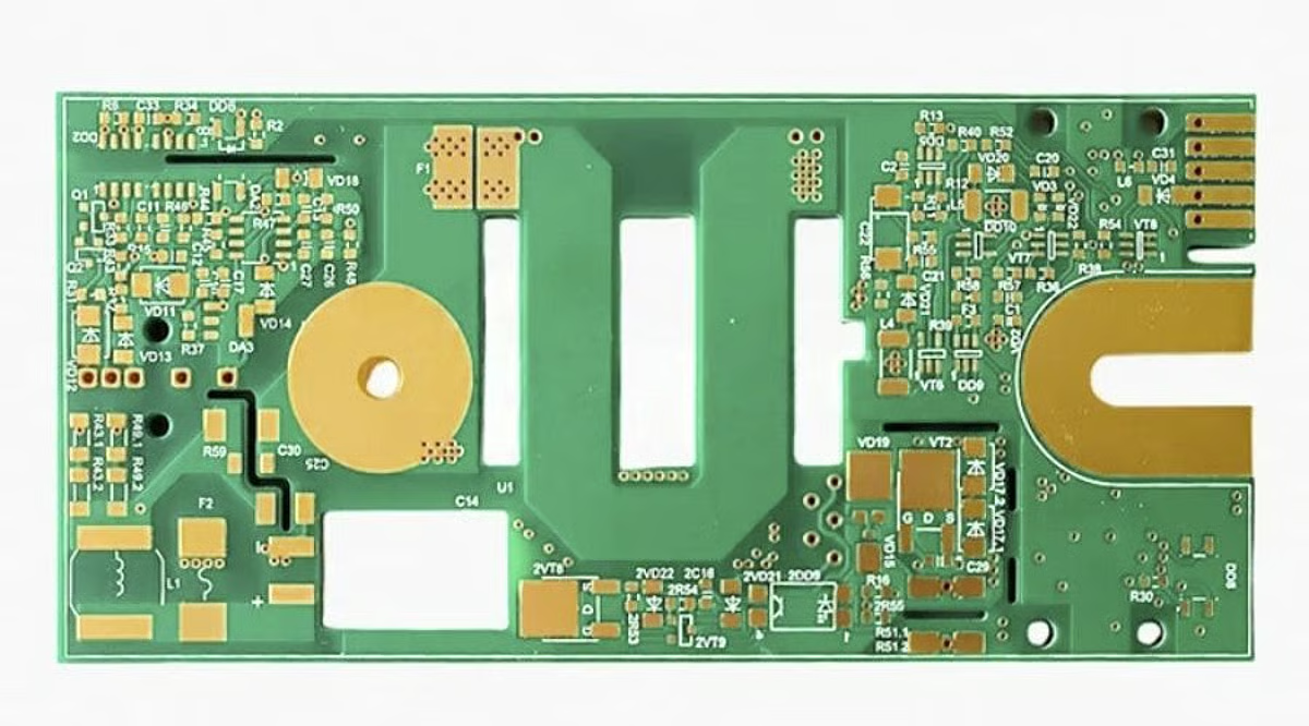
You can’t cheat physics. Electricity flows like water, and high current is a high-volume flood. If you force that flood through a narrow pipe, you get massive resistance. In a PCB trace, that resistance manifests instantly as heat.
It comes down to simple I²R losses (Joule heating). Pushing 30–50 A through a standard 1 oz trace turns your conductor into a heater. You face voltage drops, thermal stress, and eventually, delamination.
Most of us engineers reference ampacity, which is strictly tied to the cross-sectional area of the copper. A recent IEEE power electronics study on a 200 kW inverter design kept trace current density below ~5 A/mm² specifically to prevent overheating. To hit that safety margin, you either need a trace that is impossibly wide, or you need to go vertical with thicker copper.
The difference in performance is staggering. Let’s run the numbers using IPC-2221A formulas:

